Main.Team4 History
Hide minor edits - Show changes to markup
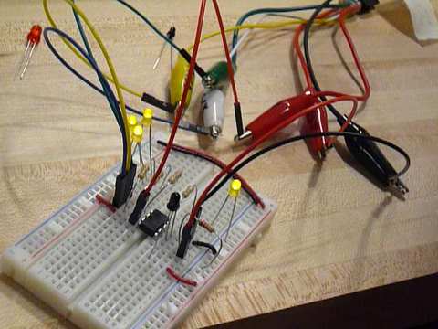
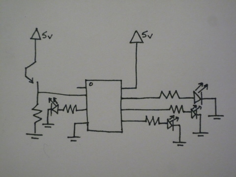
The circuit diagram shows the phototransistor at B3, and LEDs connected at B0, B1(PWM lights) B2, B4 (non-PWM) B5 is for reset and is unconnected. ( code can be found here: http://newtextiles.media.mit.edu/uploads/PmWiki/butterfly_code.txt) We first tested the layout on a breadboard before designing the actual butterfly circuit pattern.
The circuit diagram shows the phototransistor at B3, and LEDs connected at B0, B1(PWM lights) B2, B4 (non-PWM) B5 is for reset and is unconnected. ( code can be found here: http://newtextiles.media.mit.edu/2010/uploads/PmWiki/butterfly_code.txt) We first tested the layout on a breadboard before designing the actual butterfly circuit pattern.
We originally used PB5 of the AVR as the sensor pin in our prototype circuit because of location convenience. However, we got very strange behavior of the lights. It turned out that PB5 is also the reset pin, which resets the chip every time it's pulled low, which meant that every time the light turned off, the chip reset. We switched the sensor to PB3, and everything worked fine.
The day before the project was due, we were testing the chip and accidentally shorted power with ground for about 30 seconds before realizing it. Doing that killed the chip, and we were left with a butterfly with 3 LEDs that flickered erratically and wasn't responsive to light. Luckily, we had extra material and made another one. If we were to iterate on the design, we would hide the ground wire so that clipping to VCC cannot possibly touch the ground.
The circuit diagram shows the phototransistor at B3, and LEDs connected at B0, B1(PWM lights) B2, B4 (non-PWM) B5 is for reset and is unconnected. code for microcontroller We first tested the layout on a breadboard before designing the actual butterfly circuit pattern. http://newtextiles.media.mit.edu/uploads/PmWiki/butterfly_code.txt
The circuit diagram shows the phototransistor at B3, and LEDs connected at B0, B1(PWM lights) B2, B4 (non-PWM) B5 is for reset and is unconnected. ( code can be found here: http://newtextiles.media.mit.edu/uploads/PmWiki/butterfly_code.txt) We first tested the layout on a breadboard before designing the actual butterfly circuit pattern.
The circuit diagram shows the phototransistor at B3, and LEDs connected at B0, B1(PWM lights) B2, B4 (non-PWM) B5 is for reset and is unconnected. code for microcontroller We first tested the layout on a breadboard before designing the actual butterfly circuit pattern.
The circuit diagram shows the phototransistor at B3, and LEDs connected at B0, B1(PWM lights) B2, B4 (non-PWM) B5 is for reset and is unconnected. code for microcontroller We first tested the layout on a breadboard before designing the actual butterfly circuit pattern.
The circuit diagram shows the phototransistor at B3, and LEDs connected at B0, B1(PWM lights) B2, B4 (non-PWM) B5 is for reset and is unconnected. code for microcontroller We first tested the layout on a breadboard before designing the actual butterfly circuit pattern.
The circuit diagram shows the phototransistor at B3, and LEDs connected at B0, B1(PWM lights) B2, B4 (non-PWM) B5 is for reset and is unconnected. code for microcontroller We first tested the layout on a breadboard before designing the actual butterfly circuit pattern.
The circuit diagram shows the phototransistor at B3, and LEDs connected at B0, B1(PWM lights) B2, B4 (non-PWM) B5 is for reset and is unconnected. code for microcontroller We first tested the layout on a breadboard before designing the actual butterfly circuit pattern.
The circuit diagram shows the phototransistor at B3, and LEDs connected at B0, B1(PWM lights) B2, B4 (non-PWM) B5 is for reset and is unconnected. code for microcontroller We first tested the layout on a breadboard before designing the actual butterfly circuit pattern.
The circuit diagram shows the phototransistor at B3, and LEDs connected at B0, B1(PWM lights) B2, B4 (non-PWM) B5 is for reset and is unconnected. We first tested the layout on a breadboard before designing the actual butterfly circuit pattern.
The circuit diagram shows the phototransistor at B3, and LEDs connected at B0, B1(PWM lights) B2, B4 (non-PWM) B5 is for reset and is unconnected. code for microcontroller We first tested the layout on a breadboard before designing the actual butterfly circuit pattern.
The circuit diagram shows the phototransistor at B3, and LEDs connected at B0, B1(PWM lights) B2, B4 (non-PWM) B5 is for reset and is unconnected. code for microcontroller . We first tested the layout on a breadboard before designing the actual butterfly circuit pattern.
The circuit diagram shows the phototransistor at B3, and LEDs connected at B0, B1(PWM lights) B2, B4 (non-PWM) B5 is for reset and is unconnected. We first tested the layout on a breadboard before designing the actual butterfly circuit pattern.
http://newtextiles.media.mit.edu/uploads/PmWiki/butterfly_code.txt
The circuit diagram shows the phototransistor at B3, and LEDs connected at B0, B1(PWM lights) B2, B4 (non-PWM) B5 is for reset and is unconnected. code for microcontroller. We first tested the layout on a breadboard before designing the actual butterfly circuit pattern.
The circuit diagram shows the phototransistor at B3, and LEDs connected at B0, B1(PWM lights) B2, B4 (non-PWM) B5 is for reset and is unconnected. code for microcontroller . We first tested the layout on a breadboard before designing the actual butterfly circuit pattern.
The circuit diagram shows the phototransistor at B3, and LEDs connected at B0, B1(PWM lights) B2, B4 (non-PWM) B5 is for reset and is unconnected. code for microcontroller. We first tested the layout on a breadboard before designing the actual butterfly circuit pattern.
The circuit diagram shows the phototransistor at B3, and LEDs connected at B0, B1(PWM lights) B2, B4 (non-PWM) B5 is for reset and is unconnected. code for microcontroller. We first tested the layout on a breadboard before designing the actual butterfly circuit pattern.
The circuit diagram shows the phototransistor at B3, and LEDs connected at B0, B1(PWM lights) B2, B4 (non-PWM) B5 is for reset and is unconnected. code for microcontroller?. We first tested the layout on a breadboard before designing the actual butterfly circuit pattern.
The circuit diagram shows the phototransistor at B3, and LEDs connected at B0, B1(PWM lights) B2, B4 (non-PWM) B5 is for reset and is unconnected. code for microcontroller. We first tested the layout on a breadboard before designing the actual butterfly circuit pattern.
The circuit diagram shows the phototransistor at B3, and LEDs connected at B0, B1(PWM lights) B2, B4 (non-PWM) B5 is for reset and is unconnected. (((((ADD LINK TO FILE?? Program code for ATtiny13 microcontroller))))). We first tested the layout on a breadboard before designing the actual butterfly circuit pattern.
The circuit diagram shows the phototransistor at B3, and LEDs connected at B0, B1(PWM lights) B2, B4 (non-PWM) B5 is for reset and is unconnected. code for microcontroller?. We first tested the layout on a breadboard before designing the actual butterfly circuit pattern.
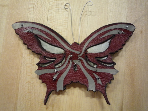
An overall (cutting schematic) was rendered with Adobe Illustrator. (((((((ADD PICTURE OF LAYOUT))))))A different image layer represents each fabric. Before cutting, it is necessary to separate the layers into discrete files in a format that can be imported to the laser cutter (ai v. 7, .dmx). Silicone molds were also created to add epoxy coatings to protect the soldered connections on the underside of the structure.
An overall (cutting schematic) was rendered with Adobe Illustrator. A different image layer represents each fabric. Before cutting, it is necessary to separate the layers into discrete files in a format that can be imported to the laser cutter (ai v. 7, .dmx). Silicone molds were also created to add epoxy coatings to protect the soldered connections on the underside of the structure.
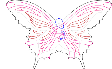
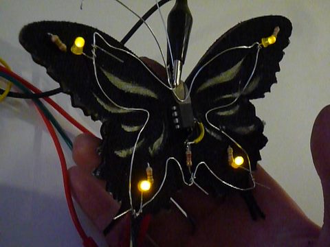
The ATtiny13 microcontroller, has 4 pins available to connect to LEDs. Two allowed for pulse with modulation (PWM) so we decided to make the layout of the LEDs symmetrical with a pair that fade on and off on the upper wings, and ones that are steady on the lower wings.
The ATtiny13 microcontroller, has 4 pins available to connect to LEDs. Two allowed for pulse width modulation (PWM) so we decided to make the layout of the LEDs symmetrical with a pair that fade on and off on the upper wings, and ones that are steady on the lower wings.
\\
\\
\\
%rframe width=400px margin-right=40px
%rframe width=400px margin-right=40px
\\
//
\\
\\
//
An overall (cutting schematic) was rendered with Adobe Illustrator. A different image layer represents each fabric. Before cutting, it is necessary to separate the layers into discrete files in a format that can be imported to the laser cutter (ai v. 7, .dmx). Silicone molds were also created to add epoxy coatings to protect the soldered connections on the underside of the structure.
An overall (cutting schematic) was rendered with Adobe Illustrator. (((((((ADD PICTURE OF LAYOUT))))))A different image layer represents each fabric. Before cutting, it is necessary to separate the layers into discrete files in a format that can be imported to the laser cutter (ai v. 7, .dmx). Silicone molds were also created to add epoxy coatings to protect the soldered connections on the underside of the structure.
\\
PCButterfly
PCButterfly
The circuit diagram shows the phototransistor at B3, and LEDs connected at B0, B1(PWM lights) B2, B4 (non-PWM) B5 is for reset and is unconnected. (((((Program code for ATtiny13 microcontroller))))). We first tested the layout on a breadboard before designing the actual butterfly circuit pattern.
The circuit diagram shows the phototransistor at B3, and LEDs connected at B0, B1(PWM lights) B2, B4 (non-PWM) B5 is for reset and is unconnected. (((((ADD LINK TO FILE?? Program code for ATtiny13 microcontroller))))). We first tested the layout on a breadboard before designing the actual butterfly circuit pattern.
\\
\\
The circuit diagram shows the phototransistor at B3, and LEDs connected at B0, B1(PWM lights) B2, B4 (non-PWM) B5 is for reset and is unconnected. (Program code for ATtiny13 microcontroller). We first tested the layout on a breadboard before designing the actual butterfly circuit pattern.
The circuit diagram shows the phototransistor at B3, and LEDs connected at B0, B1(PWM lights) B2, B4 (non-PWM) B5 is for reset and is unconnected. (((((Program code for ATtiny13 microcontroller))))). We first tested the layout on a breadboard before designing the actual butterfly circuit pattern.
Here is a video of the laser cutter scoring our circuit (it is important to cut with the paper side up - so you may have to make a reflection of your design) <object width="425" height="344"><param name="movie" value="http://www.youtube.com/v/4MdJTxC7jbI&hl=en_US&fs=1&"></param><param name="allowFullScreen" value="true"></param><param name="allowscriptaccess" value="always"></param><embed src="http://www.youtube.com/v/4MdJTxC7jbI&hl=en_US&fs=1&" type="application/x-shockwave-flash" allowscriptaccess="always" allowfullscreen="true" width="425" height="344"></embed></object>
Here is a video of the laser cutter scoring our circuit (it is important to cut with the paper side up - so you may have to make a reflection of your design) http://www.youtube.com/watch?v=4MdJTxC7jbI
Here is a video of the PCButterfly in action <object width="425" height="344"><param name="movie" value="http://www.youtube.com/v/1lFyDX-hTjA&hl=en_US&fs=1&"></param><param name="allowFullScreen" value="true"></param><param name="allowscriptaccess" value="always"></param><embed src="http://www.youtube.com/v/1lFyDX-hTjA&hl=en_US&fs=1&" type="application/x-shockwave-flash" allowscriptaccess="always" allowfullscreen="true" width="425" height="344"></embed></object>
Here is a video of the PCButterfly in action http://www.youtube.com/watch?v=1lFyDX-hTjA
butterfly_work.jpg
The circuit diagram shows the phototransistor at B3, and LEDs connected at B0, B1(PWM lights) B2, B4 (non-PWM) B5 is for reset and is unconnected. (Program code for ATtiny13 microcontroller).
butterfly_work.jpg
Here is a video of the laser cutter scoring our circuit (it is important to cut with the paper side up - so you may have to make a reflection of your design) <object width="425" height="344"><param name="movie" value="http://www.youtube.com/v/4MdJTxC7jbI&hl=en_US&fs=1&"></param><param name="allowFullScreen" value="true"></param><param name="allowscriptaccess" value="always"></param><embed src="http://www.youtube.com/v/4MdJTxC7jbI&hl=en_US&fs=1&" type="application/x-shockwave-flash" allowscriptaccess="always" allowfullscreen="true" width="425" height="344"></embed></object>
Here is a video of the PCButterfly in action <object width="425" height="344"><param name="movie" value="http://www.youtube.com/v/1lFyDX-hTjA&hl=en_US&fs=1&"></param><param name="allowFullScreen" value="true"></param><param name="allowscriptaccess" value="always"></param><embed src="http://www.youtube.com/v/1lFyDX-hTjA&hl=en_US&fs=1&" type="application/x-shockwave-flash" allowscriptaccess="always" allowfullscreen="true" width="425" height="344"></embed></object>
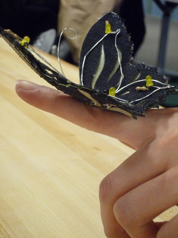
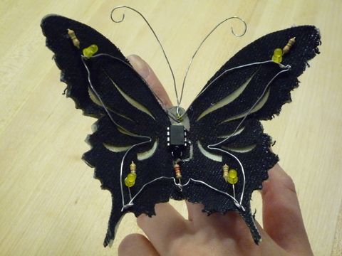
Our design is a light sensitive butterfly that turns on when in the dark. It can be easily incorporated onto clothing, bags, hair accessories etc. Our switch is a phototransistor located on the body of the butterfly design. Since the phototransistor is sensitive to changes in light it can be activated by shining and then removing the light source, yet will remain inactive in ambient light conditions. The ATtiny13 microcontroller, has 4 pins available to connect to LEDs. Two allowed for pulse with modulation (PWM) so we decided to make the layout of the LEDs symmetrical with a pair that fade on and off on the upper wings, and ones that are steady on the lower wings.
The circuit diagram shows the phototransistor at B3, and LEDs connected at B0, B1(PWM lights) B2, B4 (non-PWM) B5 is for reset and is unconnected. (Program code for ATtiny13 microcontroller). We first tested the layout on a breadboard before designing the actual butterfly circuit pattern.
There are two main fabric layers – a bottom layer for the main conductive area of the circuit, and the top layer that supports the ground wire, phototransistor, LEDs and resistors. The design incorporates iron-on adhesive conductive fabric as the substrate for the circuit. The phototransistor, LEDs and resistors are through components that source power through the microcontroller located at the center of the butterfly layout. A wire frame serves as an easily accessible ground wire as well as a structural support, which can be positioned to give the butterfly a more realistic shape. The circuit diagram shows the phototransistor at B3, and LEDs connected at B0, B1(PWM lights) B2, B4 (non-PWM) B5 is for reset and is unconnected. (Program code for ATtiny13 microcontroller).
We tested a variety of fabrics including denim, leather and lightweight lining material. We wanted to be able to incorporate a range of textures into our design and allow for easy customization by simply rearranging the materials. The lining fabric was a bit too light to use on its own reliably, although we would like to experiment more with light fabrics in the future. The laser cutter was an ideal tool for creating decorative cutout designs on the wings. Both the denim and leather provided a robust structure for our PCB and our final design included a leather underside (most of the conductive fabric was adhered to this layer), lining fabric middle layer, and a denim top layer (ground wire frame, LEDs and resistors on this side).
It is relatively easy to dislodge the soldered connections with minor manipulation. It is very useful to have a multi-meter on hand to test individual connections.
PCButterfly
PCButterfly
An overall (cutting schematic) was rendered with Adobe Illustrator. A different image layer represents each fabric. Before cutting, it is necessary to separate the layers into discrete files in a format that can be imported to the laser cutter (ai v. 7, .dmx). Silicone molds were also created to add epoxy coatings to protect the soldered connections on the underside of the structure.
Troubleshooting
The ATtiny13 microcontroller, has 4 pins available to connect to LEDs. Two allowed for pulse with modulation (PWM) so we decided to make the layout of the LEDs symmetrical with a pair that fade on and off on the upper wings, and ones that are steady on the lower wings.
[->] We tested a variety of fabrics including denim, leather and lightweight lining material. We wanted to be able to incorporate a range of textures into our design and allow for easy customization by simply rearranging the materials. The lining fabric was a bit too light to use on its own reliably, although we would like to experiment more with light fabrics in the future. The laser cutter was an ideal tool for creating decorative cutout designs on the wings. Both the denim and leather provided a robust structure for our PCB and our final design included a leather underside (most of the conductive fabric was adhered to this layer), lining fabric middle layer, and a denim top layer (ground wire frame, LEDs and resistors on this side).
'-Our design is a light sensitive butterfly that turns on when in the dark. It can be easily incorporated onto clothing, bags, hair accessories etc. Our switch is a phototransistor located on the body of the butterfly design. Since the phototransistor is sensitive to changes in light it can be activated by shining and then removing the light source, yet will remain inactive in ambient light conditions. The ATtiny13 microcontroller, has 4 pins available to connect to LEDs. Two allowed for pulse with modulation (PWM) so we decided to make the layout of the LEDs symmetrical with a pair that fade on and off on the upper wings, and ones that are steady on the lower wings.-'
The ATtiny13 microcontroller, has 4 pins available to connect to LEDs. Two allowed for pulse with modulation (PWM) so we decided to make the layout of the LEDs symmetrical with a pair that fade on and off on the upper wings, and ones that are steady on the lower wings.
[->] Our design is a light sensitive butterfly that turns on when in the dark. It can be easily incorporated onto clothing, bags, hair accessories etc. Our switch is a phototransistor located on the body of the butterfly design. Since the phototransistor is sensitive to changes in light it can be activated by shining and then removing the light source, yet will remain inactive in ambient light conditions. The ATtiny13 microcontroller, has 4 pins available to connect to LEDs. Two allowed for pulse with modulation (PWM) so we decided to make the layout of the LEDs symmetrical with a pair that fade on and off on the upper wings, and ones that are steady on the lower wings.
'-Our design is a light sensitive butterfly that turns on when in the dark. It can be easily incorporated onto clothing, bags, hair accessories etc. Our switch is a phototransistor located on the body of the butterfly design. Since the phototransistor is sensitive to changes in light it can be activated by shining and then removing the light source, yet will remain inactive in ambient light conditions. The ATtiny13 microcontroller, has 4 pins available to connect to LEDs. Two allowed for pulse with modulation (PWM) so we decided to make the layout of the LEDs symmetrical with a pair that fade on and off on the upper wings, and ones that are steady on the lower wings.-'
[->]Our design is a light sensitive butterfly that turns on when in the dark. It can be easily incorporated onto clothing, bags, hair accessories etc. Our switch is a phototransistor located on the body of the butterfly design. Since the phototransistor is sensitive to changes in light it can be activated by shining and then removing the light source, yet will remain inactive in ambient light conditions.
[->] Our design is a light sensitive butterfly that turns on when in the dark. It can be easily incorporated onto clothing, bags, hair accessories etc. Our switch is a phototransistor located on the body of the butterfly design. Since the phototransistor is sensitive to changes in light it can be activated by shining and then removing the light source, yet will remain inactive in ambient light conditions.
[->]We tested a variety of fabrics including denim, leather and lightweight lining material. We wanted to be able to incorporate a range of textures into our design and allow for easy customization by simply rearranging the materials. The lining fabric was a bit too light to use on its own reliably, although we would like to experiment more with light fabrics in the future. The laser cutter was an ideal tool for creating decorative cutout designs on the wings. Both the denim and leather provided a robust structure for our PCB and our final design included a leather underside (most of the conductive fabric was adhered to this layer), lining fabric middle layer, and a denim top layer (ground wire frame, LEDs and resistors on this side).
[->] We tested a variety of fabrics including denim, leather and lightweight lining material. We wanted to be able to incorporate a range of textures into our design and allow for easy customization by simply rearranging the materials. The lining fabric was a bit too light to use on its own reliably, although we would like to experiment more with light fabrics in the future. The laser cutter was an ideal tool for creating decorative cutout designs on the wings. Both the denim and leather provided a robust structure for our PCB and our final design included a leather underside (most of the conductive fabric was adhered to this layer), lining fabric middle layer, and a denim top layer (ground wire frame, LEDs and resistors on this side).
Our design is a light sensitive butterfly that turns on when in the dark. It can be easily incorporated onto clothing, bags, hair accessories etc. Our switch is a phototransistor located on the body of the butterfly design. Since the phototransistor is sensitive to changes in light it can be activated by shining and then removing the light source, yet will remain inactive in ambient light conditions.
[->]Our design is a light sensitive butterfly that turns on when in the dark. It can be easily incorporated onto clothing, bags, hair accessories etc. Our switch is a phototransistor located on the body of the butterfly design. Since the phototransistor is sensitive to changes in light it can be activated by shining and then removing the light source, yet will remain inactive in ambient light conditions.
- Xiao Xiao, Ellan, and Kristin
- Xiao Xiao, Ellan, and Kristin
The Concept
Our design is a light sensitive butterfly that turns on when in the dark. It can be easily incorporated onto clothing, bags, hair accessories etc. Our switch is a phototransistor located on the body of the butterfly design. Since the phototransistor is sensitive to changes in light it can be activated by shining and then removing the light source, yet will remain inactive in ambient light conditions. The ATtiny13 microcontroller, has 4 pins available to connect to LEDs. Two allowed for pulse with modulation (PWM) so we decided to make the layout of the LEDs symmetrical with a pair that fade on and off on the upper wings, and ones that are steady on the lower wings.
The Design
The Fabrics
[->]We tested a variety of fabrics including denim, leather and lightweight lining material. We wanted to be able to incorporate a range of textures into our design and allow for easy customization by simply rearranging the materials. The lining fabric was a bit too light to use on its own reliably, although we would like to experiment more with light fabrics in the future. The laser cutter was an ideal tool for creating decorative cutout designs on the wings. Both the denim and leather provided a robust structure for our PCB and our final design included a leather underside (most of the conductive fabric was adhered to this layer), lining fabric middle layer, and a denim top layer (ground wire frame, LEDs and resistors on this side).
By Xiao Xiao, Ellan, and Kristin
- Xiao Xiao, Ellan, and Kristin
PCButterfly
PCButterfly By Xiao Xiao, Ellan, and Kristin
PCButterfly
PCButterfly
PCButterfly